
Toshiba Launches 80V N-Channel Power MOSFET Using Next-Generation Process to Boost AI Data Centre Efficiency
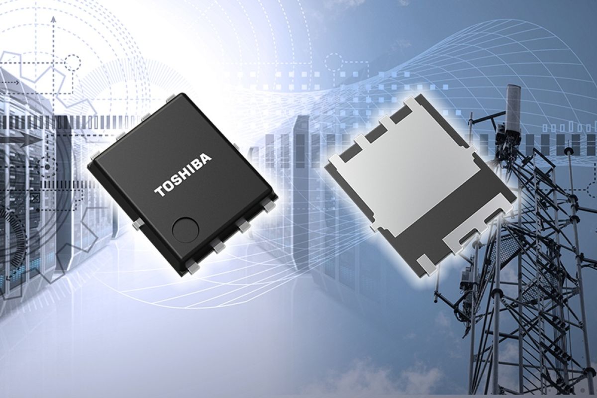
Toshiba Electronic Devices & Storage Corporation has launched the TPM1R408RH, an 80V N-channel power MOSFET manufactured using its latest generation U-MOS11-H process. The device is designed for switching power supplies in industrial equipment used in AI data centres and communication base stations. Shipments began today. As the expansion of AI processing increases power demands in data centres and advances in communications infrastructure tighten requirements for higher efficiency, smaller size, and lower electromagnetic interference (EMI) in switching power supplies, power loss directly impacts system power consumption, heat generation, and cooling loads. It is therefore essential to implement power semiconductors with characteristics that achieve a balanced reduction in conduction and switching losses, contributing to overall system optimisation including improved EMI suppression, thermal design, and ease of installation. The TPM1R408RH features an optimised device structure and achieves a drain-source on-resistance of 1.4 mΩ (max.), approximately 26% lower than Toshiba’s previous 80V product, the TPM1R908QM, which was produced using the earlier U-MOS X-H process. The product also improves the balance between drain-source on-resistance and total gate charge, achieving an approximately 45% reduction in the performance index compared to the TPM1R908QM. This characteristic represents an industry-leading low power loss level. The TPM1R408RH also suppresses voltage spikes that occur between the drain and source during switching, helping to reduce EMI in switching power supplies. EMI suppression often requires modifications at late design stages, but suppressing device-originated voltage spikes helps reduce the need for such modifications and simplifies filter and snubber circuitry. The new product uses the SOP Advance(E) package, which has approximately 65% lower package resistance and 15% lower thermal resistance compared to Toshiba’s current SOP Advance(N) package. By suppressing heat generation and improving heat dissipation, the package supports higher output and more compact power supply designs. Toshiba also provides circuit design support tools for switching power supplies. In addition to the G0 SPICE model, which verifies circuit functions in a short time, a high-accuracy G2 SPICE model that accurately reproduces transient characteristics is now available. Using the online circuit simulator on Toshiba’s website, users can easily verify circuit operation via a web browser without preparing a simulation environment or downloading device models. Toshiba will continue to expand its lineup of power MOSFETs that improve power supply efficiency, contributing to reduced power consumption in industrial equipment.